
Fabrication of nanoscale photonic crystals with ultrafast laser
KNOXVILLE, TN, October 17, 2023 /24-7PressRelease/ — Photonic crystal structures have excellent light control properties and are hot topics in the field of photonics. For the preparation of photonic crystal structures with nanoscale three-dimensional spatial resolution inside the crystal, new femtosecond laser processing technologies are urgently needed. Scientists in China proposed a photonic crystal structure fabrication method based on nanoscale femtosecond laser multi-beam lithography. The technique will open possible ways to fabricate nanostructures for applications in optical communication and light manipulation.
The light control performance of photonic crystals is closely related to their lattice constant, which typically requires the lattice constant to be in the same order of magnitude as the working wavelength. In crystal materials, the photonic crystal structure is formed by the periodic arrangement of units with different dielectric constants than the crystal itself in space, and its lattice constant depends on the size of the unit and the gap between adjacent units. Therefore, to achieve light control in the near-infrared and visible light range, it is necessary to precisely control the photonic crystal unit structure and gap at the nanometer scale.
Femtosecond laser can directly fabricate three-dimensional micro-nano structures inside transparent materials, which is one of the best ways to construct photonic crystal structures in crystal materials. However, the existing femtosecond laser processing technology for photonic crystals usually adopts a single-beam point-by-point scanning strategy, which is limited in the preparation of nanoscale unit structures due to the overlapping of processing trajectories and motion control accuracy. Micro-lens array processing technology and laser interference processing technology provide solutions to the above problems to a certain extent. However, the former is not flexible enough, and different micro-lens arrays need to be designed and fabricated for different target structures. Although the latter has high flexibility, it can usually only be used to process flat two-dimensional structures, lacking three-dimensional customization ability. Therefore, new femtosecond laser processing technology is urgently needed for the preparation of nano-scale three-dimensional spatial photonic crystal structures inside crystals.
In a new paper published in Light Science & Application, a team of scientists, led by Professor Lan Jiang from School of Mechanical Engineering, Beijing Institute of Technology, Beijing 100081, China, developed a method for fabricating photonic crystal structures based on nanoscale femtosecond laser multi-beam lithography by tightly focusing a multi-beam light field with controllable three-dimensional spatial distribution inside a crystal and combining it with chemical etching. On one hand, the size and gap of the fabricated structural units can be controlled at the sub-wavelength level by designing the optical phase and tight focusing method. On the other hand, the use of a multi-beam light field allows for optical control instead of electrical control, effectively avoiding problems such as laser spot overlapping and precision of component movement that exist in single-beam laser processing.
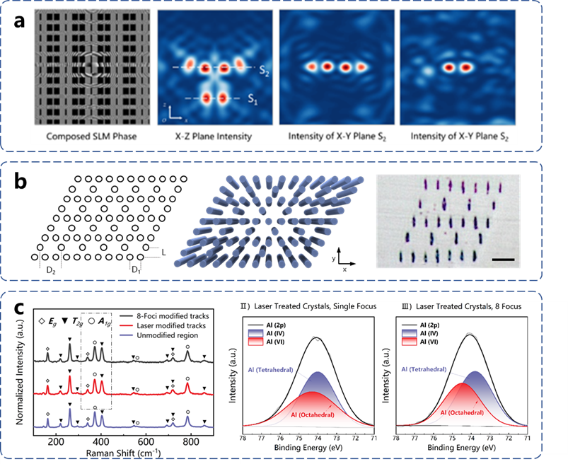
The one-to-one correspondence between spatial phase and the distribution of the light field provides feasibility for this method. In this article, researchers found that the binary phase period and laser flux jointly affect the size and gap of the processed structure, and realized the preparation of sub-wavelength scale photonic crystal structure units. Based on the above result, by adjusting the grayscale of the binary phase and the superposition method of the final phase, the multi-beam light field with controllable laser flux distribution and three-dimensional spatial structure can be customized, and the corresponding complex structure photonic crystal can be processed. Raman spectroscopy and X-ray photoelectron spectroscopy tests indicate that the structural units obtained by this processing method are the same as the results of single-beam point-by-point scanning under non-overlapping states, with high stability and reliability. Using this method, long-period and sub-wavelength grating structures were prepared, and experimental test results were consistent with theoretical calculations, further verifying the processing ability of this method.
These scientists summarize the advantages and perspective of their technique:
” (1) Simple operation and low cost, without the need to design different optical components for processing different target structures; (2) Precise control of structure dimensions and gaps enables the fabrication of photonic crystal unit cells at the nanoscale; (3) Three-dimensional complex spatial structure processing capability enables the preparation of three-dimensional photonic crystal structures inside the crystal.”
“The flexible control over nanostructures makes the reported method an alternative to weave complex photonic crystals with subwavelength structure. The potentials of multi-beam processing method may open possible ways to fabricate nanostructure for applications in optical communication and light manipulation.”
References
DOI
10.1038/s41377-023-01178-3
Original Source URL
https://doi.org/10.1038/s41377-023-01178-3
Funding information
This work is supported by the National Natural Science Foundation of China (Grant No. 52075289)
Contact
Lan Jiang. School of Mechanical Engineering, Beijing Institute of Technology, Beijing 100081, China, [email protected]
About Light: Science & Applications
The Light: Science & Applications will primarily publish new research results in cutting-edge and emerging topics in optics and photonics, as well as covering traditional topics in optical engineering. The journal will publish original articles and reviews that are of high quality, high interest and far-reaching consequence.
Chuanlink Innovations, where revolutionary ideas meet their true potential. Our name, rooted in the essence of transmission and connection, reflects our commitment to fostering innovation and facilitating the journey of ideas from inception to realization.
Related Link:
http://chuanlink-innovations.com
—
For the original version of this press release, please visit 24-7PressRelease.com here